


Results 1 to 3 of 3
-
12-24-2014, 10:05 AM #1Administrator

- Join Date
- Jan 2014
- Posts
- 7,697

Researchers Use Novel Additive Manufacturing Technique Called Nanoshaping
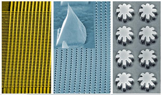
It's an entirely new method of “additive manufacturing” where the only thing added is 1 or 2 gigapascals of force. It might better be called 3D stamping, but by using “laser shock imprinting,” the process creates 3D crystalline metallic structures as small as 10 nm with ultrasmooth surfaces – and it does so at room temperature. Researchers from Purdue University and a couple other institutes of higher learning came together to pioneer the new technique, and it seems to have potential to bring 3D printing down to the nanoscale. Check out more details: http://3dprint.com/31221/laser-shock-imprinting/
-
12-24-2014, 12:32 PM #2Technician
- Join Date
- Feb 2014
- Location
- NJ
- Posts
- 65
Very interesting. It is amazing to see how metal Additive Manufacture is not just being used for the very big (aircraft parts, etc.) but also for the nano scale. I wonder if the researchers used a AFM (Atomic Force Microscopy) machine to do this. The resolution and "benchtop" elements would make sense. Would be very cool to look at the actual paper (It's Science so an institutional subscription or pay per article is needed).
Thanks for sharing!Last edited by ajperez; 12-26-2014 at 09:37 AM.
-
12-24-2014, 12:50 PM #3Super Moderator
- Join Date
- Jul 2014
- Posts
- 8,818
should be useful for external devices and characteristics on nanobots.


 Reply With Quote


Extruder not feeding during print,...
Yesterday, 01:59 AM in Tips, Tricks and Tech Help