


Results 1 to 1 of 1
Hybrid View


-
04-18-2017, 04:07 PM #1Administrator

- Join Date
- Oct 2016
- Posts
- 2,028
Researchers Develop Hydroprinting Technique
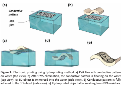
A lot of focus has been placed in recent years on producing 3D structures with conductive features, particularly in terms of the Internet of Things. The difficulty that arises when attempting to print conductive structures onto 3D objects comes from the sometimes uneven and complex topography of substrates, which makes it difficult to deposit liquids onto the surface. Researchers from The Hebrew University of Jerusalem and the Nanyang Technological University in Singapore recently published a paper which presents their method of using a hydroprinting process to fabricate conductive circuits and patterns. Read more at 3DPrint.com: http://3dprint.com/171609/hydroprint...tive-patterns/

 Reply With Quote


Print not sticking to base plate?
Yesterday, 01:26 PM in General 3D Printing Discussion